Removing the pain of advanced process node NAND error correction with BENAND™ from Toshiba
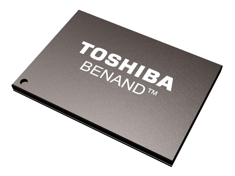
BENAND™, the SLC NAND Flash Memory with Built-in Error Correction Code (ECC)
As NAND Flash memory moves towards more advanced process nodes, the cost of devices is reduced but the cells become more vulnerable to program/erase stresses. The new technology requires more Error Correction Code (ECC) to maintain the desired levels of data integrity. Unfortunately, many chipsets or controllers are unable to perform more than 1-bit or 4-bit ECC. BENAND™, an SLC-NAND with built-in ECC, takes this challenge away from the controller. This paper describes how BENAND™ can be smoothly integrated into industrial and other applications – substituting the legacy SLC NAND with the latest advanced technology without the need to change the host system.
NAND Flash is used in a wide variety of industrial, communication, automotive and consumer devices requiring non-volatile storage for code, data or content. To respond to market demands for lower costs and increased storage capacity, fabrication technology is advancing quickly to each successive new process node. This strategy is successful in achieving the small die sizes and high memory densities needed to satisfy market demand.
With every gain there typically comes a challenge, however. In the case of deep nanometre NAND Flash, smaller process geometries bring demands for increased error- correction. This is necessary to guarantee reliability in line with expectations and system demand.
As with standard NAND Flash, regardless of process geometry, issues such as high-voltage stress during program/erase cycles can alter or damage individual cells. Over time the number of affected cells increases. The only way to manage this gradual deterioration is to perform error correction on all data read from the device and to avoid using known affected cells. At smaller process nodes, the individual cells are more susceptible to failure induced by high-voltage stress.

Figure 1a and 1b: Falling cost of NAND Flash and rising ECC overhead with advancing process technology.
To date, more error correction has been needed for Multi-Level Cell (MLC) NAND technology, while Single-Level Cell (SLC) NAND has typically required only 1-bit ECC for densities up to 4Gb fabricated at 4Xnm. A 1-bit ECC algorithm is defined as being able to correct one failure bit per 512 bytes. The latest small density SLC NAND Flash devices, fabricated at 3Xnm or 2Xnm, require 4-bit or 8-bit ECC, respectively, per 512 bytes. Figure 1a and 1b contrast the cost-down advantages of advanced process technologies with the associated increases in ECC complexity.
For many existing applications that use SLC NAND memory, such as industrial designs, communication processors and automotive systems, the 1-bit ECC is implemented in the host software with no significant effect on application performance. Migrating to ‘cutting-edge’ memories that require 4- or 8-bit ECC would significantly increase processor workload. To avoid processor performance bottlenecks, a hardware-based ECC has become the preferred solution.
BENAND™ – The Alternative to Standard Raw SLC
Recently, in the case of the latest SLC NAND solutions, a new option has become available to the designer, namely BENAND™ (Built-in ECC NAND) memory, which features an embedded ECC function.
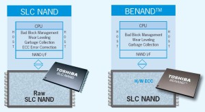
As figure 2 illustrates, BENAND™ removes the burden of ECC from the host processor without requiring an additional hardware controller. It is important to note that BENAND™ uses the common NAND interface, thereby ensuring compatibility with general SLC NAND Flash in areas such as command set, device operation, packaging and pin configuration. As indicated in figure 2, issues such as bad-block management and wear levelling are handled in the same way as with raw SLC NAND.
BENAND™ technology allows OEMs to benefit from the reduced cost and increased memory density associated with smaller process geometries, whether in completely new designs or when migrating existing applications to more advanced memory solutions. An existing design can be migrated without changing established hardware.
Performance Comparison
The effective speed of BENAND™ is comparable to that of raw SLC NAND. Although BENAND™ in fact has longer read (tR) and program (tPROG) times, due to the internal ECC, the host-side ECC needed for raw SLC would add the same – or longer – delay.
BENAND™ delivers valid data, correcting errors due to failed memory cells. The system is normally unaware of the physical condition of the NAND cells. Sending a Status Read command causes the BENAND™ to report if a page contains corrected or incorrectable cells. This information can be utilised in the memory management on the host system.
Design-in and Compatibility
If BENAND™ is used to replace a standard SLC NAND in an existing application, best performance can be achieved by disabling any ECC performed by the host. If host ECC cannot be turned off, the BENAND™ will continue to provide error-free operation using its own built-in ECC.
A common question from developers relates to the availability of a second source, particularly when a new category of devices is revealed. As BENAND™ is compatible with SLC NAND, SLC NAND could be used as a second source for BENAND™.
BENAND™ devices are packaged as standard TSOP-I-48-P and 63-ball BGA devices, which are pin compatible with known SLC packages. In addition, Toshiba offers a very small 6.5mm x 8.0mm 67-ball BGA version. This is ideal for use in new designs for extremely space-constrained applications. Today BENAND™ is available with 1Gbit to 8 Gbit density.
BENAND™ is a trademark of Toshiba Corporation.
Find BENAND™ on our Rutronik24 Online Shop.

