Infineon – CoolSiC™ MOSFET in Easy 1B, 2B for EV charging
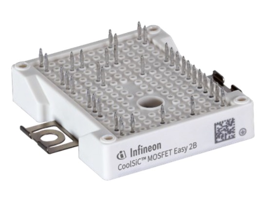
F4-23MR12W1M1_B11 and F3L15MR12W2M1_B69
Combining the strengths of two great Infineon products: the Easy package, a benchmark in low stray inductance and the 1200 V CoolSiC™ MOSFET enables customers to significantly reduce their system and operational costs.
With regard to topology, these products meet the demand for EV charging applications such as high-frequency operation and large output variation of the DC-DC power stage.
Features
– CoolSiC™ MOSFET in Easy package for lowest stray inductance
– Superior gate-oxide reliability
– Enables higher fsw operation due to nearly 80% lower switching losses compared to Si
– Intrinsic diode with low reverse-recovery charge
– Highest threshold voltage of Vth > 4 V
– Multiple switches in the small Easy package for a very compact solution
– CoolSiC™ MOSFET as an addition to Infineon’s extensive chip portfolio
Benefits
– Operation at higher switching speeds up to 50 kV/μs
– Longer lifetime of converter system
– Reduced system and operational costs due to high efficiency and reduced cooling effort
– Increased power density
– Highest robustness against parasitic turn-on
– Easier system integration and reduction of manufacturing effort
– Optimized hybrid module solutions for individual converter topologies
Competitive advantage
> Flexibility for inverter designs due to different available topologies
Target applications
– EV-Charging
Diagram
Product overview incl. data sheet link
| Rutronik Number | Type | SP Number | OPN | Package |
| IGBT2662 | F4-23MR12W1M1_B11 | SP001710600 | F423MR12W1M1B11BOMA1 | EASY1BM-2 |
| IGBT2663 | F3L15MR12W2M1_B69 | SP001710612 | F3L15MR12W2M1B69BOMA1 | EASY2BM-2 |
Product collaterals / Online support
– Product page F4-23MR12W1M1_B11
– Product page F3L15MR12W2M1_B69
– Video
– Article: Electric Vehicle Fast Charging Challenges

